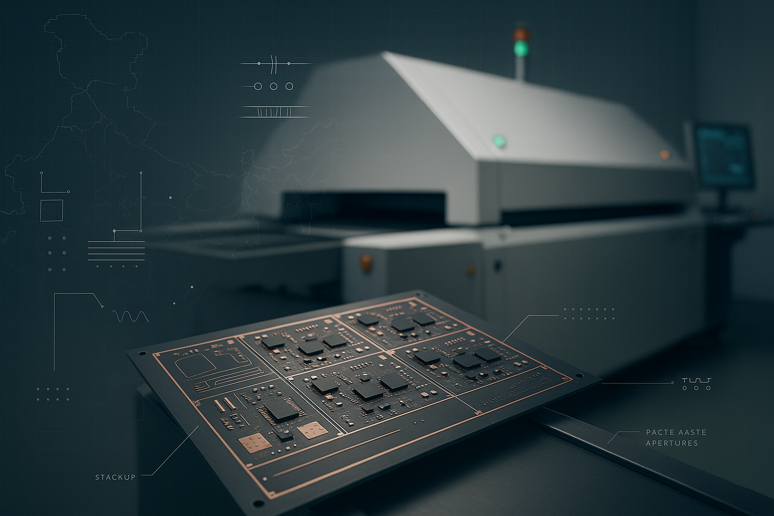
Flying probe tester(FPT) is used during the final stages of PCB (Printed Circuit Board) manufacturing process to test and validate the functionality of circuit boards. In a bare PCB, this would mean testing defects such as opens and shorts. Flying probe tester has been in the industry for quite some time and is still popular in today’s manufacturing world.
A netlist along with the solder mask information is fed to the flying probe testing software which determines the test points and the path for navigation of the probes on the machine. Then the bare PCB is inserted to the machine. Three points on the board are marked in the software for calibration. The machine now maps the features on the Gerber with the features on the physical board, it forms a 1:1 mapping. Now, the machine is ready to test the board.

The test begins with four robotic probes initially performing a homing sequence and then move to different locations on the board defined in the test point file and verifies with the netlist for any open circuit present in the board. Once all the points are covered, it then checks for the presence of shorts. Two probes are present on the top side of the board and two are on the bottom side, this accelerates the test time. When all the test points are covered, the software indicates if all the points on the board passed the electrical testing, in case of defects it will point the location of the defect along with the type of defect.
Each board manufactured in LionCircuits facility goes through a set of tests including the FPT. In addition to FPT, a new AI-based optical inspection machine from Tooling AI is used in production which detects anomalies well in advance in the manufacturing process. Tooling AI machine is also used in defect detection of assembled circuit boards. We will cover the details of Tooling AI machine in another article.
AI is the new electricity and it’s already changing the manufacturing industry. We at LionCircuits use AI/ML in various process and our platform learns with every iteration.
.png)
%20(1).png)


