Modern electronics manufacture depends on castellated holes in printed circuit boards (PCBs), a necessary component with special benefits for several uses. Along PCB's edge, these half-plated holes form a connection point for additional PCBs or components.
Usually found in surface mount technologies (SMT) and modular PCB designs, castellated holes provide simple and consistent connections. They enable flawless integration of several modules, hence enabling scalable and flexible electrical architectures.
A proper knowledge of its features will improve the efficiency and usefulness of designs, This article seeks to give a thorough knowledge of castellated holes covering their design, production technique, and advantages for electronics producers.
Key Highlights
- Castellated holes are half-circle holes that run along the edges of a printed circuit board (PCB), making a solid connection point for soldering parts.
- The main advantages of castellated holes are easy integration and better reliability.
- While designing castellated holes, manufacturers must maintain proper space between holes, consult experts, use specialised software, and ensure perfect alignment.
- Castellated Holes manufacturing goes through various steps like drilling, plating, cutting, finishing, and quality control.
- Castellated holes play a significant role in the manufacturing of electronic parts like connectors, modular components, breakout boards, etc.
What are Castellated Holes?
Castellated holes, which are also called metal half-holes, are half-circle holes that run along the edges of a printed circuit board (PCB).
By plating the inside of the holes and then cutting the PCB through them, a number of half-plated holes are made that give the design its own look.
In real life, they look like holes or cuts on the edges of the PCB. Castellated holes work as both electrical and mechanical connections to connect modular parts.
Electrically, they make a solid connection point for soldering parts or other PCBs, making sure that signals and power are sent and received efficiently. Mechanically, they provide strong anchoring places that make the structure of the modules stronger when they are put together.
Since they can do two things, castellated holes are very useful in many situations where stable performance and easy integration are important. This includes modular PCB designs and surface mount technology (SMT).
By using castellated holes, designers can make flexible, strong, and scalable electronic systems that meet the strict needs of modern electronics.
Why are Castellated Holes Important?
Advantages in the Design of PCBs:
- Easy Integration of Modules: Castellated holes make it possible to link multiple PCB layers in a seamless manner. It simplifies the assembly process and reduces the amount of intricate cabling that is required.
- Enhanced Reliability: These holes offer robust mechanical bonds and dependable electrical connections. That’s why it guarantees consistent performance even in applications that are particularly demanding.
Specific Cases to Consider
- Castellated holes are good for prototyping. Because they make it simple to test and troubleshoot individual modules prior to final assembly. This makes them a perfect choice for small-scale production.
- Certain modules in applications require frequent updates or modifications. Castellated holes make it possible to easily replace or upgrade them. This eliminates the need to rebuild the complete printed circuit board (PCB).
Design Requirements for Castellated Holes
1) Diameter and Spacing
Make sure there is enough space between castellated holes. It protects the structure from shorting out and helps to avoid short circuits. Standard hole diameters are usually between 0.4mm and 0.6mm. But this can change based on the PCB design and the parts that are being used.
2) Alignment
Exact alignment of the castellated holes is necessary for the links to work fine. If things aren't lined up right, the solder joints and electrical links may not function right. During the planning process, use alignment guides. Also, fiducial marks help to make things more accurate. Follow the IPC-7351 guidelines. It gives detailed rules for how to place castellated holes and makes sure that the end product is compatible and improves its reliability.
3) Consult Experts
Talk to PCB manufacturing experts to find out about special features and restrictions they have on castellated holes. Manufacturers may have specific needs for spacing, hole plating, and standards. They need to be taken into account in the design.
4) Software Tools
Use PCB fabrication and design tools like Altium Designer, Eagle, or KiCad. They have features just for making holes with multiple levels. These tools help automate things like spacing, alignment, and following standards. This speeds up the planning process and lowers the chance of making mistakes.
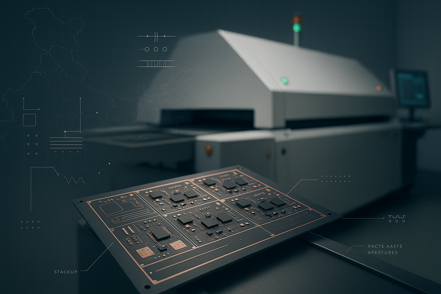
Manufacturing Process of Castellated Holes

1) Drilling:
Make holes in the PCBs edge. This is where castellated holes should be placed. Also, make sure the holes are placed precisely to avoid mismatch. For that, use CNC drilling tools that are very accurate.
2) Plating:
Use an electric current to coat the inside of the holes made with copper. Copper will connect electricity wires. To make sure links work, make sure the plating thickness is the same all over. Use controlled coating baths and keep an eye on them often.
3) Cutting:
To make the half-circle, castellated holes, cut the PCB through the plated holes. Keep the cuts clean and exact without damaging the plated surfaces. For precision, use high-tech ways to cut, like CNC milling.
4) Finishing:
Use HASL, OSP, or ENIG PCB to finish the surface. It will cover the copper that is showing and make sure that it can be soldered well. Make sure the finish sticks well to the edges that were cut. Before putting on the finish, make sure the PCB is completely clean and ready.
5) Quality Control:
Check for flaws like odd plating or holes that aren't lined up right by visually inspecting and using machines to do so. Do electrical tests to make sure the connections work and the structure is strong. Set up strict rules for quality control and use tools like X-ray analysis to do a full check.
Design Considerations for Castellated Holes
1) Pad Design
In order to design PCB pads, people should make sure that they are somewhat larger than the hole. By doing so, it will provide an adequate soldering area as well as mechanical stability. If anyone wants to improve the development of solder fillets, use pads that are rectangular or rounded rectangular.
2) Hole Size
Measure the diameter of the hole, which should be between 0.4 and 0.6 millimetres. Always take into consideration the particular requirements of the application when determining the size. Make sure that the hole size is compatible with the components as well as the capabilities of the production process.
3) Surface's Finish
Producers should choose a surface finish that is suitable for the job, such as HASL, ENIG, or OSP. A surface treatment that is of the highest quality will protect the exposed copper and increase its solderability. ENIG is frequently chosen because of its exceptional dependability and longevity.
4) Obtaining Certifications
Certifications such as RoHS, UL, and ISO9001 should be upheld to ensure compliance. As a result, businesses are able to reach the criteria for quality, safety, and the environment. To ensure that the design is in accordance with these requirements, consumers should collaborate with certified manufacturers.
5) Pad Array on Main Board
Create the pad array that will be located on the first board. It will be helpful in matching the castellated holes in order to achieve optimal integration and connections that are reliable. To guarantee that the positioning is appropriate, designers should make use of alignment markers and precise measurements.
Applications of Castellated Holes
The uses and patterns show the adaptability and significance of castellated holes in modern electronic items..
1) Modular Components
Help modular PCB components to be integrated into bigger systems. Perfect instances for such are Wi-Fi and Bluetooth chips found in Internet of Things devices.
2) Connectors
As strong links between several PCBs, connectors improve mechanical stability and electrical connectivity. For this, pay special attention to interfacing main control board sensor modules.
3) Breakout Boards
Activate simple microcontroller pin and other small component access on breakout boards. It will ease testing and prototyping. Breakthrough boards for Arduino and Raspberry Pi will help for the same.
4) Real-World Products
Castellated holes can be used for modular design and small-scale integration, consumer electronics including wearables, smart homes, and cellphones regularly make use of castellated perforations.
5) Emerging Trends and Future Prospects
Growing use in sophisticated uses include automotive electronics, tiny medical devices, and 5G modules. Demand for castellated hole technology will be driven by ongoing IoT and smart device growth, therefore encouraging more PCB design and manufacturing innovation.
Conclusion
Castellated holes are an important part of designing and making modern printed circuit boards (PCBs). Because they have many benefits, such as making it easier to integrate modules, improving stability, and having many uses in many different areas. Using these half-plated holes makes sure that the connections are strong. Along with that, they speed up the PCB assembly process in many situations, from making prototypes to making market electronics. As technology changes, shaped holes are becoming more and more important in printed circuit board (PCB) projects. These holes make the design more flexible and the PCB work better. In order to get more detailed information or help from experts, talk to people who work in the field or look at other resources.