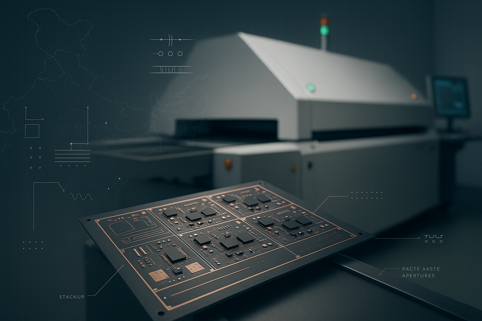
%20(1).jpg)
Integrations are often the secret behind all the fast and reliable electronic devices. To reduce the size of applications, their inner components need to be more slim and efficient than traditional ones. Engineers use HDI PCB as their integrated circuit board to achieve this goal in different sectors. With the help of key features like micro vias, blind and buried vias, more fine lines and spaces, accurate sequential lamination, and advanced via-in-pad techniques, these circuit boards offer smooth performance that lasts for years. It is one of the reasons that a wide spectrum of industries, such as healthcare, automotive, or even wearable applications, are increasingly choosing this multilayer PCB.
In this blog, all the information about advanced HDI PCBs will be discussed in detail, from what it does to where it is used. Knowing these boards will allow consumers to better inspect their products before purchasing.
Key Highlights
- High-Density Interconnect (HDI) board is an advanced type of printed circuit that has a higher wiring density per unit area compared to traditional PCBs.
- HDI PCB designs can accommodate a higher density of PCB components than standard ones.
- You must create enough stack-ups, do impedance matching and ensure the quality of material as well as manufacture to design a high-quality HDI PCB.
- The HDI PCB manufacturing process involves many steps like material selection, multi-layer stack-up, photolithography, etching, microvia drilling, plating, lamination, solder mask application, surface finishing, assembly, and final inspection.
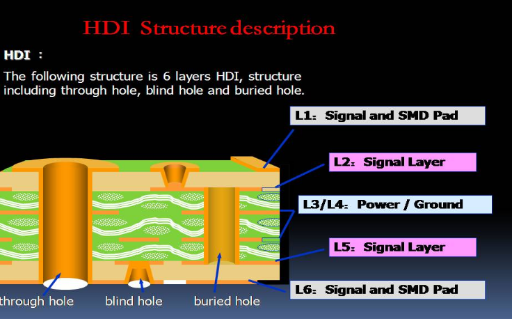
- The various types of vias in HDI PCBs are through-hole vias, buried vias, blind vias, and microvias.
- Some of the key benefits of HDI PCBs are improved density, performance, efficiency, and cost-effectiveness.
- HDI PCBs are used in many industries like healthcare, smartphones, automotive, military, and aerospace.
What defines an HDI board?
A High-Density Interconnect board is an advanced type of printed circuit board. HDI PCBs have a higher wiring density per unit area compared to traditional PCBs.
The design specifications for HDI boards are outlined in IPC-2226, which sets the standard for intricate electronic connections. It also has a unique design specification for HDI boards.
For instance, on an HDI board, the fine lines and spaces are less than or equal to 100 microns or 0.10 mm. And their small vias are, in general, less than 150 micrometres. For the capture pads, the designated size is less than 400 microns or 0.40 mm.
The striking feature of these boards is their higher connection pad density. On a typical HDI board, there are more than 20 pads per square centimetre.
To talk about the different types of HDI available on the market, they are named Type I, Type II, and Type III. Each of them is uniquely different in terms of complexity and performance.
Type I HDI boards are the simplest among all the other variants. They mostly use a single buildup of high-density interconnection layers. Type I is found in simpler applications.
On Type II boards, two or more HDI layers are used. The best part is that engineers can optimise the space as per their requirements.
And Type III HDI boards are the most complex in design. These boards contain three or more sequential build-up layers. It allows the boards to accommodate the highest density of components. It is one of the reasons that the most demanding electronic applications choose this last type of HDI board.
What is HDI PCB Design?
HDI PCB designs can accommodate a higher density of PCB components than standard ones. Since modern electronic items are slowly becoming more compact, this design helps a lot.
HDI PCB design typically includes careful planning of the stack-up, micro-via structures, and signal integrity. Stack-up planning is essential to optimise electrical performance without the need for a large space. Along with that, microvias reduce the PCB size and improve the integrity of signals.
To achieve optimal performance in HDI PCBs, following a specific design is required. For example, designers often use a fanout strategy from complex ICs. It allows them to limit space and make each pin accessible.
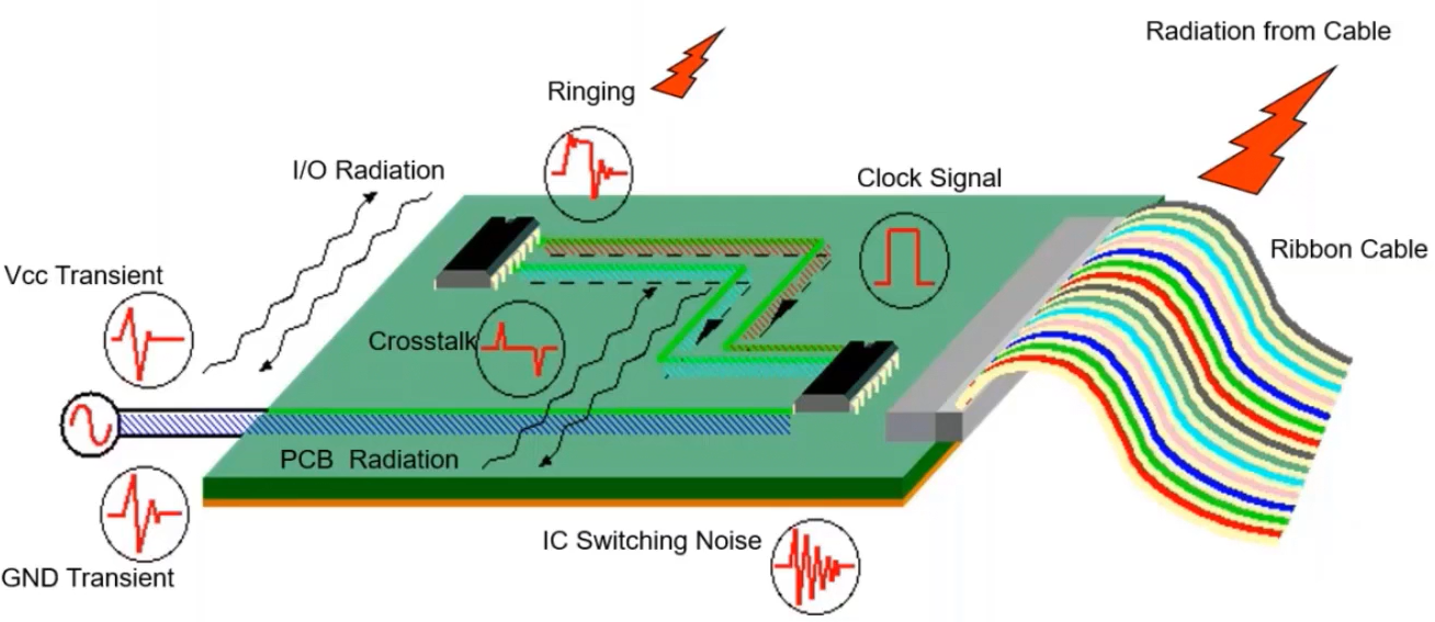
Crosstalk often becomes a common challenge in densely packed circuits. To omit that, designers must consider the number of sequential layers. Increasing the number of layers can enhance performance. However, It also raises the cost and complexity of manufacturing.
Designing HDI PCBs can become challenging due to their complex structure. Balancing component density with signal integrity often ends up being too difficult to handle. If it is not done carefully, the high component density can lead to noise issues during improper signal transmission. Also, due to the latest technology used in manufacturing, the cost rises.
Design Guidelines for HDI PCB
A careful balance between technical requirements and production capabilities is the key design feature of High-Density Interconnect PCBs. Here are some guidelines for that:
- Similar to other PCB variants, such as single-sided PCBs, the manufacturer's ability also plays a pivotal role here. Ensure the manufacturer's capability to deal with HDI technology, including fine line widths, microvias, and high layer counts, before finalising the design.
- One difficulty that arises during production is signal delays. To avoid or minimise the risk, creating an efficient stackup helps. It can effectively reduce the lengths of signal paths. Thus, it also helps manage the routing of dense interconnects. Designers should aim for a stackup that is both cost-effective and meets the electrical performance criteria.
- Additionally, impedance matching is also essential to prevent signal reflections. Designers need to be careful while drafting layout and routing to mitigate crosstalk and electromagnetic interference.
- The quality of the substrate and conductive layer, along with a choice of PCB gold fingers, has a significant role in determining the durability and efficiency of this circuit board.
HDI PCB Manufacturing Process
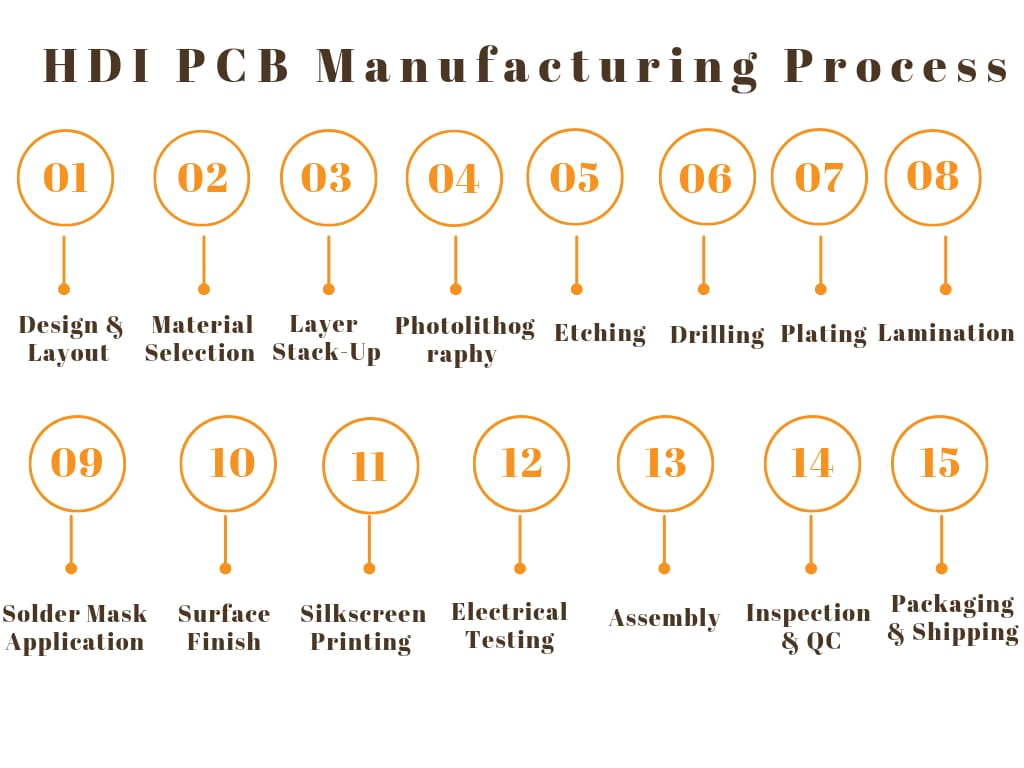
Step 1: Design and Layout
To start the product, first create a detailed schematic design and layout. Using Computer-Aided Design (CAD) software may help in this regard. In this step, components and routing traces are placed accurately to ensure optimal functionality.
Step 2: Material Selection
Then choose the appropriate substrate. A high-quality fibreglass or similar material will work best. Along with that, copper foil is the best choice of conductive layers.
Step 3: Layer Stack-Up
Determine the number of layers needed for the HDI PCB. Then design the stack-up. It outlines the arrangement of conductive and insulating layers. This ensures that the circuit board can handle the complex routing and connectivity required.
Step 4: Photolithography
Apply a photoresist material to the substrate. After that, expose it to UV light through a mask that defines the circuit pattern. Thus, the board is prepared for the etching process.
Step 5: Etching
Etch away the unwanted copper using a chemical solution, leaving behind the desired circuit pattern. Repeat this process for each conductive layer. It will create a precise and accurate circuit path on the PCB.
Step 6: Drilling
Use a laser to drill microvias. These tiny holes will connect different layers of the PCB. For larger vias, mechanical drilling is required.
Step 7: Plating
In the next step, a thin layer of copper is applied in the drilled holes. Then, the copper layer is thickened through electroplating.
Step 8: Lamination
To make the board sturdy, lamination is used. Laminate the layers together using heat and pressure.
Step 9: Solder Mask Application
Then a solder mask layer is applied to protect the copper traces and prevent short circuits. It enhances the reliability and performance of the finished PCB.
Step 10: Surface Finish
To protect the exposed copper areas against oxidation and improve solderability. A surface finish is performed. One popular circuit board that uses a surface finish is ENIG PCB.
Step 11: Silkscreen Printing
During this process, the component labels, logos, and other necessary markings are printed on the PCBs. This step leads to smooth assembly and testing.
Step 12: Electrical Testing
Performing electrical tests will minimise any risk of errors in the connections. Automated optical inspection and other testing methods are often used to verify the integrity and functionality of the board.
Step 13: Assembly
In this step, the components on the PCB are placed using automated pick-and-place machines and then soldered the components onto the board.
Step 14: Final Inspection and Quality Control
After assembly, conducting one final visual inspection is necessary. It will reveal any potential defects during the manufacturing process. This step ensures that only high-quality, fully functional boards are shipped to the customer.
Step 15: Packaging and Shipping
This is the final process. Cleaning the PCB to remove any residues from the manufacturing process is highly important. After that, they are carefully packed in protective packaging. Thus, businesses can ensure damage-free shipping.
To talk about the cost, HDI PCBs can be comparatively inexpensive in certain applications. Although advanced technologies like laser drilling and direct laser imaging are indeed costly, they are cost-saving in the long run. The functionality this PCB fabrication process achieves at the end of the process is unmatched, which justifies the initial higher investment.
Types of Vias in HDI PCB
Several types of vias are used in high-density interconnect PCBs. These variables play a critical role in achieving the desired success. Learn the different types of vias here:
- Through-Hole Vias: These are the most traditional types of vias. From the top to the bottom of the PCB, a hole is drilled. Moreover, they connect multiple layers in a multi-layer PCB. These types of vias are relatively easy to manufacture. Hence, they are cheaper as well.
- Blind Vias: These vias are more advanced than through-hole vias. This also connects an outer layer of the PCB to one or more inner layers. However, they do not go all the way through the board. Blind vias are more complex to produce. Hence, they are more expensive than through-hole vias. Designers choose them when space is more limited and no broad surface is available to drill holes.
- Buried Vias: Do you not want to let the vias be visible from the outside? Buried vias are created to provide just that. They connect the internal layers of a PCB without being visible from the surface. These vias are completely hidden within the board. Inside two or more internal layers, these vias may present depending upon the requirements.
- Microvias: Compact designs require smaller components. Microvias are the smallest type of bias among all their different counterparts. Microvias generally have a diameter of less than 150 microns. And just like through-hole vias, they can be drilled with laser technology. They are essential for modern electronics, where advanced technology comes in miniature.
Benefits of HDI PCBs
Compared to traditional PCBs, HDI PCBs are more efficient. These high-density interconnected PCBs use advanced technology. It also allows for more inclusive designs for the applications. The key benefits of HDI PCBs are:
- Increased Density: HDI PCBs can support more connections per unit area. According to their specific guidelines, they can hold more than 20 PCB pads per square centimetre. Thus, these boards can integrate more components. This is particularly beneficial for modern electronic devices because these devices are compact but perform highly.
- Improved Performance: Due to the use of microvias in HDI PCBs, the electrical paths become shorter. It also reduces the risk of signal loss. Thus, the boards can send away faster signals at faster transmission rates. For high-frequency applications, HDI PCBs become more reliable.
- Enhanced Design Efficiency: With the use of HDI PCBs, designers can place components closer together. Thus, the connections become more smooth for transmission. It also simplifies the design and PCB assembly processes.
- Reduced Weight and Size: Since there has to be no other layer, the design of the application becomes more compact, and the weight drops as well. Moreover, HDI PCBs are lighter and thinner. Thus, they safely get fitted in mobile and wearable technology.
- Cost-Effective in the Long Run: Compared to traditional PCBs, these high-density interconnected PCBs are more costly. However, since they are more reliable and run longer, these initial investments become justified. Hence, the applications become cost-effective in the long run. Also, due to mass production, the price was reduced further.
Applications of HDI PCBs
High-Density Interconnect PCBs are integral parts of numerous sectors. They are highly efficient and offer impressive performance. Here is a list of all the industries using HDI PCB.
- Healthcare: HDI PCBs are crucial for the development of life-saving devices like pacemakers. These devices need to be reliable. More than that, they have to be miniature. To perform critical diagnosis efficiently, medical devices choose paramount components like HDI PCB.
- Automotive: The sensors and infotainment systems in the automotive industry generally have limited space. HDI boards come in handy to suit compact designs. Along with that, they are also integral to autonomous vehicles. These boards can transmit complex and high-speed signals, thus maintaining vehicle functionality.
- Smartphones and Tablets: For slim and lighter designs, smartphones also need HDI PCBs. These circuit boards add necessary multifunctionality to their high-resolution screens and multiple cameras.
- Wearable Technology: HDI PCBs can also be found in smartwatches and fitness trackers. These devices are small in size and offer high performance. Thus, these advanced PCBs become part of these wearables.
- Military and Aerospace: Military and aerospace applications are advanced and use HDI PCBs as well. These PCBs are also reliable for sending continuous signals. Thus, these advanced printed circuit boards become an integral part of communication systems and navigational controls.
Conclusion
HDI PCBs are transforming the electronics industry. With a more compact and efficient design, they are being used in high-performance devices. Similar to other PCBs, such as RF PCBs, a high-performing circuit board becomes necessary to optimise device performance across different industries. For those involved in electronic design and manufacturing, exploring the potential of HDI PCBs will open opportunities for new growth.