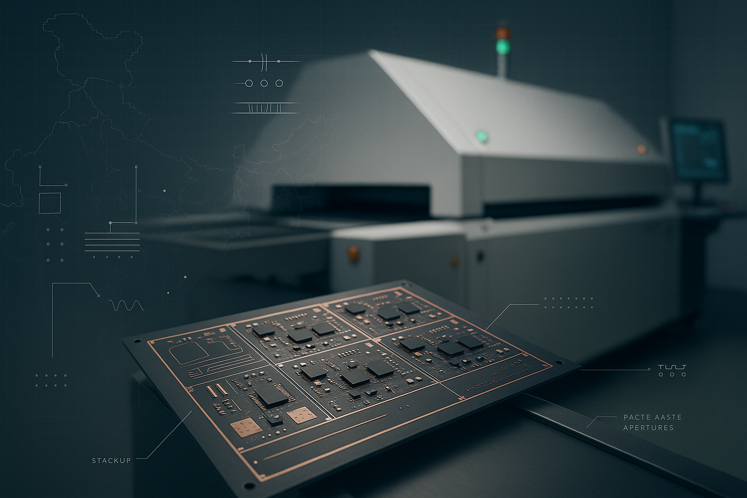
Every Printed Circuit Board (PCB) has gold-plated connectors that are attached to its edges, called PCB gold fingers. It is the top-notch connector in the PCB industry because of its metallic plating. For PCs, game consoles or industrial equipment, it is fundamental to have PCB gold fingers that guarantee reliable connections and good performance. This post will cover all aspects of PCB Gold Fingers starting from their specifications to how they can be used.
Key Highlights
- PCB gold fingers are gold-plated connectors that can be found on the edge of printed circuit boards (PCBs).
- Some of the crucial factors while designing gold fingers are the width of the finger, inter-gold finger gap, accuracy in lining up, length of the finger
- PCB edge connectors are typically long and narrow strips along the PCB edge while gold fingers are small, flat, gold-plated terminals at PCB edge
- PCB beveling is an essential process for gold fingers to improve the durability and functionality of PCBs.
- PCB gold fingers are used in a variety of sectors like telecommunication, industries, computers, etc.
What Are PCB Gold Fingers?
PCB gold fingers are gold-plated connectors that can be found on the edge of printed circuit boards (PCBs). These connectors can facilitate smooth connections between PCBs and other components or systems like expansion cards or motherboards, PCI Express, PCI, AGP Cards, etc.
The main function of PCB gold fingers is to provide a strong and low-resistance connection point that can withstand repeated insertions and removals. These PCB components are made of a thick nickel coating followed by a thin gold coating. Gold is being used due to its excellent properties for conductivity, corrosion resistance, and wear resistance, ensuring long-lasting performance. Usually, the gold plating ranges from 3 to 50 microinches thick, depending on the application's durability requirements.
PCB Gold Fingers Specifications
PCB's technical specifications are highly divergent. These manufacturing processes differ based on the thicknesses of gold, individual manufacturing requirements and conformity to different standards. This is why some issues must be taken into consideration when designing a gold finger. Some of the crucial factors are the width of the finger, inter-gold finger gap, accuracy in lining up, length of the finger as well as others. While the specifications of gold fingers may differ depending on the situation, three fundamental guidelines should consistently be followed:
- Gold-plated connectors cannot coexist near plated-through holes.
- Keep solder masks and screen printing away from gold fingers.
- When bevelling the PCB edge, ensure that the gold fingers don't face towards the middle of the PCBs.
Neglecting these rules can cause damage to the gold finger, leading to disconnectivity between the components and the circuit boards.
While gold is a durable metal, it is costly and unsustainable. Therefore, to further strengthen the gold, nickel is used before it is electroplated. The ideal nickel electroplating thickness should be between 150 and 200 microinches. The Association Connecting Electronics Industries (IPC), came into existence in 2002 to globalise the use of gold fingers worldwide. Consequently, IPC-4556 (2012) was released followed by IPC A-600 and IPC-6010 in 2015 which have turned out to be guidelines for PCB assembly worldwide since their publication. Below is a concise overview of the IPC standards:
- Chemical composition: To Strengthen the edge connectors of the PCB, cobalt should be added to the alloy mixture of Electroplating gold. Cobalt should comprise at least 5% but no more than 10% of the mixture.
- Plating Thickness: Electroplating should ideally range from 2 to 50 microinches in thickness, depending on its purpose. Standard thicknesses for different applications include 0.031, 0.062, 0.093, and 0.125 inches.
- Visual test: A visual test is needed to identify any potential damages using a magnifying lens. Edges should be inspected thoroughly and the surface finish must be smooth.
Tape test: Since the surface finish is electroplated, a tape test needs to be conducted. A white tape strip is placed along the edges and then it is pulled off to see any signs of gold plating.
PCB Gold Fingers vs PCB Edge Connectors
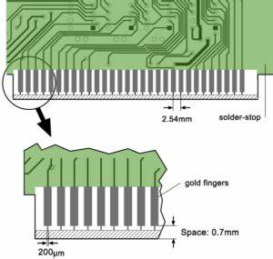
What is PCB Gold Finger Beveling?
The PCB fabrication process starts before the surface finish and after the application of the solder mask. The process consists of three steps. These are as follows:
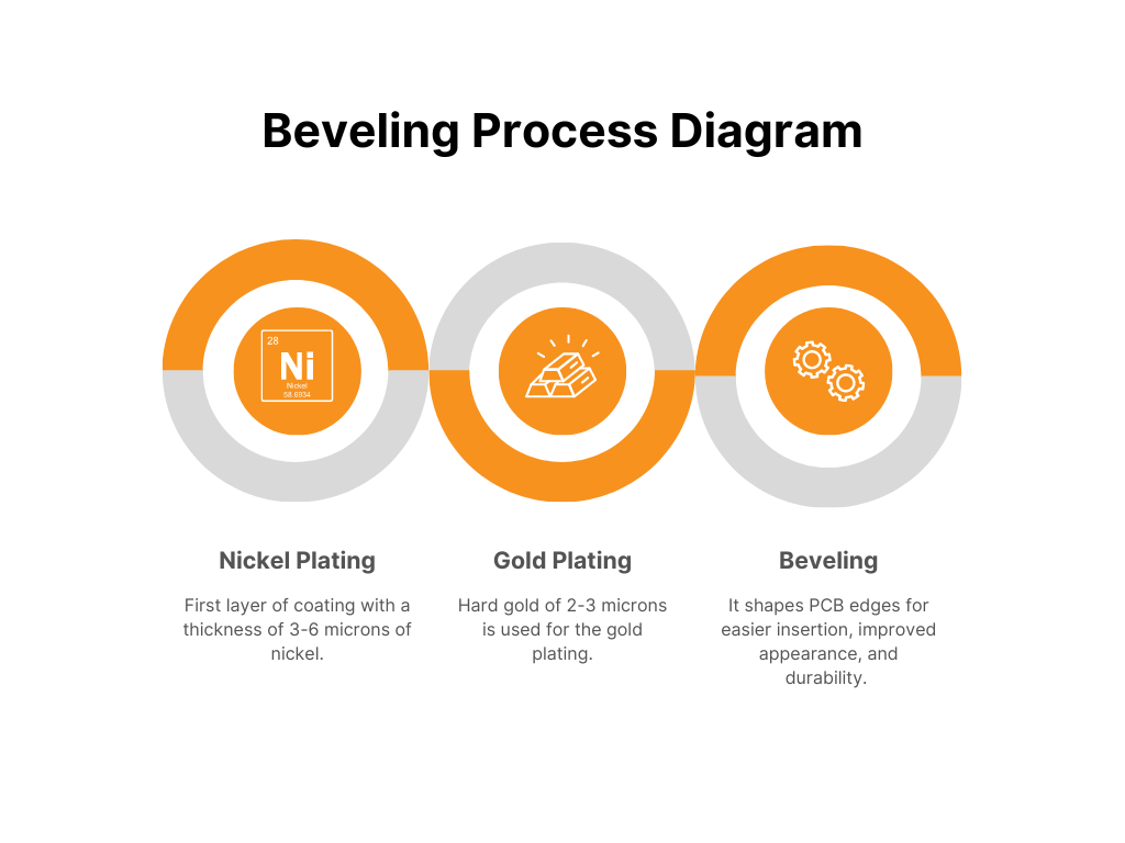
- Nickel Plating: This is the first layer of coating with a thickness of 3-6 microns of nickel.
- Gold Plating: Hard gold of 2-3 microns is used for the second layer of plating. Here gold is mixed with cobalt for maximum rigidity and surface resistance.
- Beveling: Lastly PCB gold finger beveling shapes PCB edges for easier insertion, improved appearance, and durability. Typically angled at 30 degrees, beveling must never exceed 45 degrees.
This process is essential for gold fingers, since beveling enhances the durability and functionality of PCBs, particularly in applications requiring frequent plugging and unplugging.
Design Specifications and Rules of PCB Gold Fingers
Many PCBs can have longer gold fingers and can be inserted into long slots. Since it can break easily, the plating of components requires some rules to be followed:
- Inner PCB layers must be copper-free to prevent exposure when beveling.
- Avoid PTH within 1 mm of Gold Fingers.
- Maintain at least 0.5 mm distance between gold fingers and board outline.
- Any compromise in spacing can weaken the PCB.
- No solder mask or printing near Gold Fingers.
- Gold Fingers should face outwards from the PCB centre.
How Are PCB Gold Fingers Used?
After PCB assembly, the boards serve as the backbone of today’s electronic devices, channelling energy and facilitating communication between various components. Here are some common usages of PCB gold fingers:
- Telecommunication application: They are used as expansion slots (like PCI and AGP) for high-speed data transfer.
- Computer application: Memory modules, such as RAM sticks, employ gold fingers for reliable connections. Peripheral devices like graphics cards and network interface cards also use them for interface stability.
- Industrial application: Additionally, in industrial equipment, gold fingers are employed in control systems and instrumentation for their durability and conductivity.
Final Thoughts
Nowadays, more advanced technologies are coming up to the surface rapidly along with the usage of electronic devices. These devices rely on PCB gold fingers for smoother connectivity. There are many materials used for the PCB layer, however, using gold along with nickel can offer more durability and better performance. In retrospect, the design and the manufacturing process of PCB gold fingers can make all the difference. It is important to ensure that gold fingers are tested and plated properly to the highest standards. So before starting your next PCB project, keep these factors in mind.