Ever since the development of technology, devices are getting smaller day by day. Almost all prominent brands feature compactness and lightweight as Unique Selling Propositions (USPs). So, as the devices are aiming to get smaller, traditional welding tools like soldering iron may not be of much use. That's where the relevance of PCB stencils comes in.
In this blog, important topics like what is a PCB stencil, how it is manufactured, types of stencils, and how to use them, will be discussed.
Key Highlights
- PCB stencil refers to a stainless steel sheet that has precise openings.
- Main types of PCB Stencil are: framed stencils, frameless stencils, hybrid stencils, and electroformed SMT stencils.
- In order to create PCB stencils, manufacturers must select the right materials, cut the holes. Inspect the stencil, and perform stencil framing and stencil printing.
- Generally, PCB stencils are reusable depending on various factors like quality of materials, type of stencil, thickness, storage, and cleaning process.
- Usage of PCB stencils must be done in the presence of professionals with proper safety gears and gloves.
What is a PCB stencil?
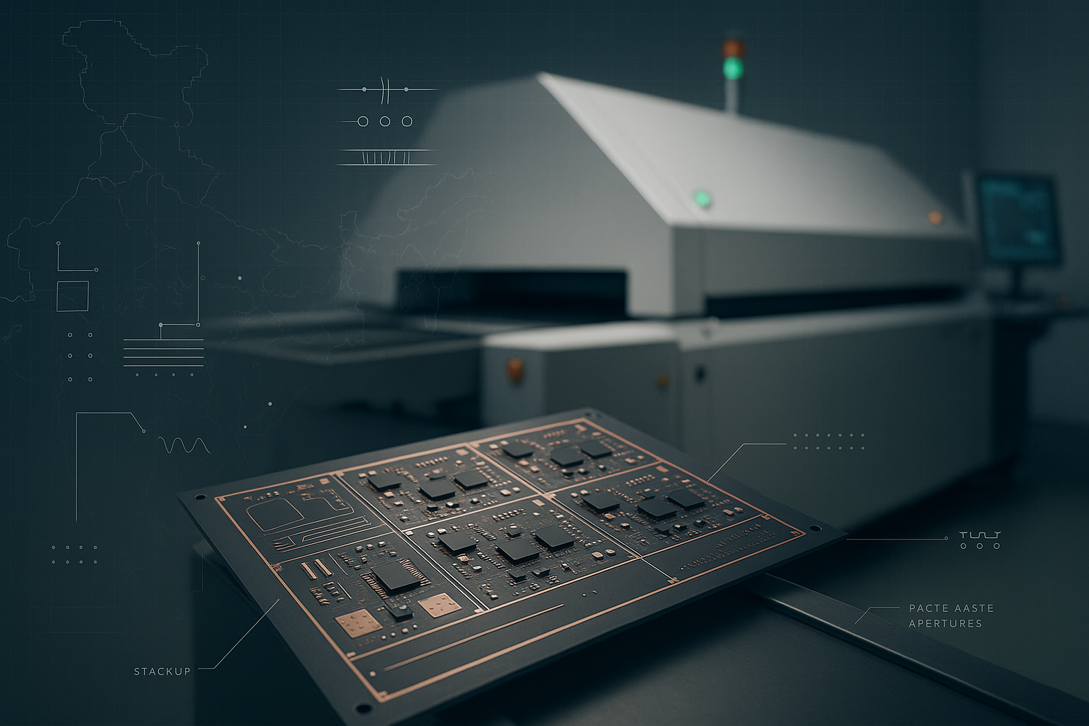
PCB stencil refers to a stainless steel sheet that has precise openings. They are used to place solder paste onto various fixed spots on a board after the PCB fabrication process. Metals that have higher durability like stainless steel, nickel, etc., are used in its manufacturing.
The precise cut-outs in PCB stencils are called apertures. They are created using sophisticated techniques like laser cutting, to match the exact measurements of the solder pads on the PCB.
Types of PCB Stencils
There are various types of PCB stencils, depending on the mounting and opening type. Some of the prominent ones are:
There are various types of PCB stencils, depending on the mounting and opening type. Some of the prominent ones are:
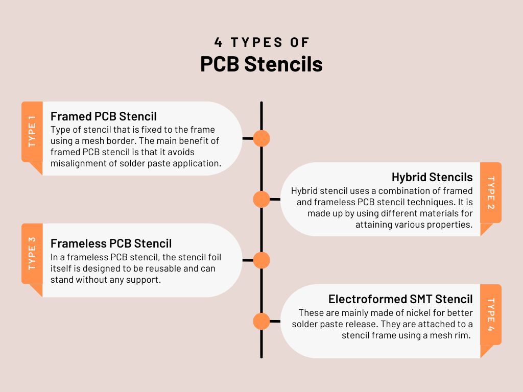
1. Framed PCB Stencil
Framed PCB Stencils refer to the type of PCB stencil that is made for screen-printing processes. It is also called glue-in stencil. As the name suggests, the stencil is fixed to the frame using a mesh border. The main benefit of framed PCB stencil is that it avoids misalignment of solder paste application.
2. Frameless PCB Stencil
In a frameless PCB stencil, the stencil foil itself is designed to be reusable and can stand without any support. Therefore, any kind of traditional frame is not used. As a result, the cost of producing frames can be saved.
3. Hybrid Stencils
Hybrid stencil uses a combination of framed and frameless PCB stencil techniques. It is made up by using different materials for attaining various properties. For example, a stencil for delicate electronic components could use a combination of a heat-resistant Kapton film for laser cutting intricate shapes and a stainless steel frame for rigidity during PCB etching.
4. Electroformed SMT Stencil
Apart from other stencil types, these are mainly made of nickel for better solder paste release. They are attached to a stencil frame using a mesh rim.
Manufacturing Process of PCB Stencil and How to Use It
Many techniques are used in the production of PCB stencils. Check out the most commonly used procedures:
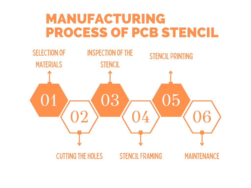
1. Selection of Materials
First of all, identify the places where surface-mount components are to be placed and prepare a design for the PCB stencils. After approving the design, a stainless sheet is to be taken as the raw material. Alternatively, long-lasting materials like Nickel, Polymer, or even plastic could be used, depending on the budget.
2. Cutting the Holes
Precise apertures are created on the PCB stencils using various techniques. Many manufacturers opt for the laser cutting process in which a high-powered laser beam is used to cut the designed aperture patterns into the stencil foil.
3. Inspection of the Stencil
The PCB stencil is keenly cleaned to clear any remains of the aperture process. A quality check is made by PCB assembly professionals to make sure that it releases paste in the optimum quantity during the printing process.
4. Stencil Framing
In case the company is producing a framed stencil, it is to be framed with sturdy material to ensure proper alignment and it gets fixed firmly. This step is not required for a frameless PCB stencil.
5. Stencil Printing
The stencil is placed on the top of the PCB in accordance with the markings in the design. Now, place a metal squeegee blade at the starting point of the print stroke and apply pressure downwards to ooze out the paste through the apertures to the solder pads.
6. Maintenance
The application of solder paste is not the end process. Manufacturers must regularly clean it and perform check-ups to ensure that it works as per the standards.
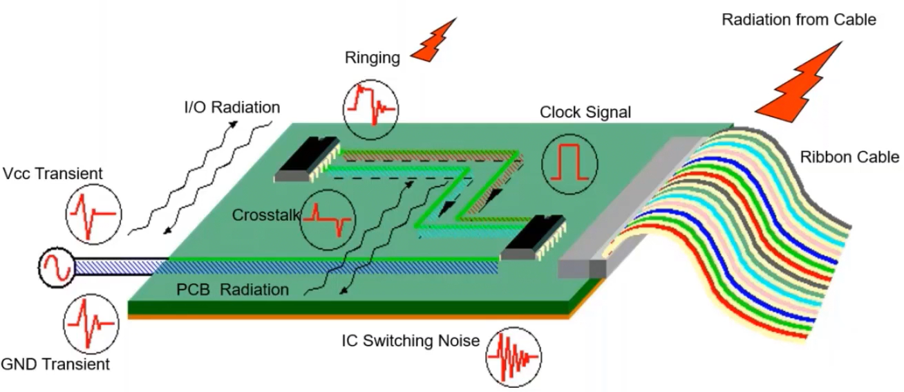
Significance of Pads in PCBs
PCB pads pave the pathway for component placement in a PCB. Therefore, the quality of PCB pads has a direct stake in the overall effectiveness of stencils. Here are the key points about the significance of pads in PCBs:
- Pads are designed to be slightly larger than the corresponding stencil to ensure proper alignment.
- Pads serve as the touchpoints for connecting components and the traces on the PCB.
- PCB pads make sure that the solder joints are reliable and the electrical connections last for a long time.
- The thickness of the pads must be optimal to prevent overflow of solder.
- Pads ensure that components work in safer temperatures as they help in effective heat dissipation.
- Surface mount pads allow the placement of more components over a specific area, facilitating space saving.
Are PCB Stencils Reusable?
Generally, PCB stencils are reusable as they are made up of long-lasting materials like stainless steel. However, there are many limitations. Check out some factors that determine the reusability of a PCB stencil:
- Material Quality: if the stencil is made of premium quality materials such as stainless steels of 301/304 grade, stencils are more reliable.
- Thickness: Generally, stencils that are thicker are likely to sustain more.
- Size of Solder pads: Stencils with larger solder pads have longer durability.
- Type of Stencil: Damage to stencil edges is a common phenomenon during stacking. Framed stencils help to tackle this situation to a large extent.
- Cleaning Process: if the company manages a team of professionals to conduct regular cleaning and check-up processes, the stencil may last longer.
Storage Process: environmental factors like dust, humidity, heat, etc., have a stake in the durability. If the stencil is stored in sealed moisture barrier bags, life expectancy gets longer.
Best Practices While Using PCB Stencils
Since stencils are complex PCB components, errors during usage are quite common even with expert manufacturers. However, it could be avoided to a great extent by following these guidelines:
- The process must be held in the presence of professionals who have experience in aligning the stencil with the PCB using fiducial marks.
- Before the placement, ensure that the stencil does not have any blockages or damage.
- Labourers must wear gloves and proper safety gear to avoid exposure of the surface to contaminants.
- Clean the stencil using ultrasonic agitation or any other advanced technique to make sure that there are no residuals after the process.
- In case the manufacturer wants to reuse the stencil in the future, it must be stored in a flat and dry environment, covered with a protective film to avoid contact with dust.
Final Words
Stencils are one of the most important components during the PCB assembly process as they play a key role in ensuring the proper functioning of electric devices. It helps to prevent many problems like misalignment, excess application of paste, etc. Getting the best protection requires not only an in-depth understanding but also perfect execution of PCB stencil procedures from experts.