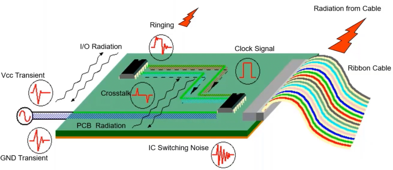
Cross Talk:
When you dealing within High Speeds tracks, it is important to make sure that your critical tracks do not become the aggressor or the victim. The first step to achieving this is to space tracks well among themselves on each layer. This is where rule-based softwares such as Altium, Mentor Graphics, Etc., have a sufficient advantage over software that is freely available and may not provide a rule/constraint based PCB routing. In traditional low voltage design, a spacing of about 20 mils between single-ended tracks would be just enough. And would be a logical compensation between noise mitigation and your tracks taking a reasonable amount of space. But this will vary from the engineer to engineer and design to design, so make sure that you use software approximations to understand what would work best for you. Next, we move to the interlayer stack up. Your tracks can couple capacitively to any signal within the same layer it can also couples easily with tracks that are in the adjacent layers if the distance between the layers is small. It is beneficial to have an un-cut “reference plane” as close as possible to the high-speed signal layer. This also gives a short and complete return path of your electric fields between tracks, this is how the reference plane acts as both a shield and a low impedance path for return currents to flow back to the chip. Having a reference plane very close to the high-speed layer will also help you to drastically reduce the track spacing that you require to keep your SI good and within your tolerance.
Return Paths:
Watching you return current is by far one of the most important points to take care in high-speed design.
Every signal that is going into any port carries a finite amount of current, it could be in mA, μA or even Pico-Amps. This is what defines the conventional circuit theory of how circuits work.
When your tracks switch at high frequencies, the parasitic capacitance becomes a concern. At high frequencies, the impedance of a capacitor lowers, and at some point, the impedance reduces to an extent that the return path is right on the ground plane (reference plane) and anti-parallel to the track on the top layer. This is why having an uncut solid reference plane (usually system GND) is most important to maintain a low impedance and a proper return path of the system. When analyzing return paths, it is important to note that currents and voltages in digital and analog systems are very different. And they should not mix at any point to an extent that the impedance of the region is raised or the digital current move to the analog side.
.png)
One of the debates of the 21st century that has been put to rest is that “Should a system have a solid ground plane or a split ground plane?”. Folks in the late 1900s would have sworn by their trade that it’s better to keep a split ground than to go for a single ground. Fast forward, in the 21st century, you see a there is a radical shift in what electronics designers are doing right now and there is plenty of data that you should be better off with a solid ground in your mixed signal system all throughout.
So why is there such a radical shift in perspective of these well thought out designers?
It’s all boils down to return currents again!
Let’s take for example a low frequency, high sensitive ADC, (the ones that are used to measure data an ECG of course) and perhaps with 24bits of precision. In ADCs, the chip is divided into two independent sections, a digital section, and an analog section. When the system is operational the goal of the designer is to isolate the digital noise (peaky and unstable) away from the analog sections (however possible). They can do (in theory) this easily by dividing the section into an analog ground and a digital ground and connecting only at perhaps a single point on the board. This can in effect, raise the impedance/resistance of the return path and keep the digital noise from coupling into the analog section. This is very well justified in theory, except for that fact that the analog and digital sections within the ADC can interact internally and couple noise into the analog section if you do not provide a better low impedance return path outside the chip.
Enter the solid ground plane, when you have a solid ground plane, both the digital and analog grounds are tied together with the least impedance that is possible.
So how do we do achieve better performance with a solid ground plane than a split one?
Well this trick here to be super careful with the placement of component that encompasses the digital and analog sections of your board. Placement is of paramount importance as a designer it is your responsibility to make sure that there would be no digital (or some crisscross high current return that may introduce a drop even in the order of uV) return paths crossing the analog section. The can make or break your board design.
So what we learned about split ground planes was all a lie?
Well no, split ground planes are kind of okay when you have multiple ADC on the same board that have to work simultaneously side by side to each other. Sectioning ground planes, when you have multiple ADCs, makes sure that no analog return current from one ADC goes into the analog section of another ADC. This is the best cases alternative for better SI in this scenario.
.jpg)
.jpg)
Many ADCs and DACs have separate analog ground (AGND) and digital ground (DGND) pins. On the device data sheets, users are often advised to connect these pins together at the package. This seems to conflict with the advice to connect analog and digital ground at the power supplies, and, in systems with more than one converter, with the advice to join the analog and digital ground at a single point.
There is, in fact, no conflict. The labels, “analog ground” and “digital ground,” on these pins refer to the internal parts of the converter to which the pins are connected and not to the system grounds to which they must go. For an ADC, these two pins should generally be joined together and to the analog ground of the system. It is not possible to join the two pins within the IC package because the analog part of the converter cannot tolerate the voltage drop resulting from the digital current flowing in the bond wire to the chip. But they can be tied together externally.
Figure 3 illustrates this concept of ground connections for an ADC. If these pins are connected in this way, the digital noise immunity of the converter is diminished, somewhat, by the amount of common-mode noise between the digital and analog system grounds. However, since digital noise immunity is often of the order of hundreds or thousands of millivolts, this factor is unlikely to be important.
The analog noise immunity is diminished only by the external digital currents of the converter itself flowing in the analog ground. These currents should be kept quite small, and they can be minimized by ensuring that the converter outputs don’t see heavy loads. A good way to do this is to use a low input current buffer at the ADC output, such as a CMOS buffer-register IC.
.jpg)
If the logic supply to the converter is isolated with a small resistance, and decoupled to analog ground with a local 0.1-μF (100-nF) capacitor, all the fast-edge digital currents of the converter will return to ground through the capacitor and will not appear in the external ground circuit. If a low-impedance analog ground is maintained—as it should be for adequate analog performance— additional noise due to the external digital ground current should rarely present a problem.
A final piece of the puzzle is when you are designing a system for a high-speed analog acquisition. To reiterate, when you have a high-speed track going from one chip to another, the return path will most likely be on the solid ground plane beneath it. This has to do with capacitive coupling to the ground plane due to lower impedance via the ground plane. It is paramount in any design to have a solid ground plane, as close to the high-speed track as possible to facilitate a low impedance return path.
.jpg)
.jpg)
.jpg)
The third part will be released soon, where we will be talking about Track Impedance and Placement. Stay Tuned!
About the Author:
Tony is currently the Lead Hardware Design Engineer at Nymble Labs, Bangalore, India. He is a conventional electronics geek and love to indulge in anything and everything related to chips (fried and baked alike!). His experience mainly revolves around Mixed-signal design and Power electronics with a dab of High-Speed Design and EMC/EMI. In the meanwhile, he reads books and listens to podcasts that center around history and human psychology as a diversion. He often loves to geek out, and making a conversation with him is so much easier when it’s on any one of these topics.