Wave soldering is a basic operation in the fabrication of printed circuit boards that lays down a core foundation for producing dependable electrical connections. This method guarantees that every component is firmly connected to the board by running the PCB across a wave of molten solder. PCB assembly requires soldering since it offers the mechanical and electrical bonds required for the lifetime and operation of the board.
PCB manufacture uses two main soldering techniques: reflow soldering and wave soldering. Surface-mounted devices usually use reflow soldering; wave soldering is mostly used for mixed technologies assemblies and through-hole components. Particularly in high-volume production runs, wave soldering's efficiency and simplicity make it a desirable method in many different uses. Maintaining the dependability and quality of electronic goods depends on an awareness of these processes.
This blog will cover everything about wave soldering in PCB, what it is, importance of wave soldering, types of wave soldering, how wave soldering is done, applications of wave soldering and limitations.
Key Highlights
- Wave soldering is a technique used to solder through-hole components to guarantee that the solder conforms to the exposed metal surfaces of the components and the board.
- The main advantages of wave soldering are efficiency, reliability, and cost-effectiveness.
- Reflow soldering is mainly used for SMDs while wave soldering is practised for through-hole components.
- You must prepare the PCB, apply the flux, heat it, perform the soldering process, and cool it for practising wave soldering.
- You must ensure proper safety gears, consistent soldering technique, and sufficient ventilation to avoid any defects in the wave soldering process.
What is Wave Soldering?
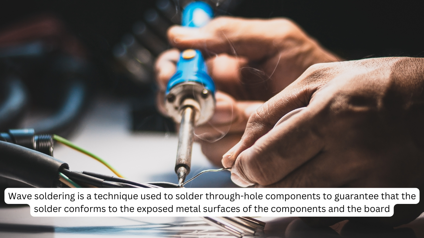
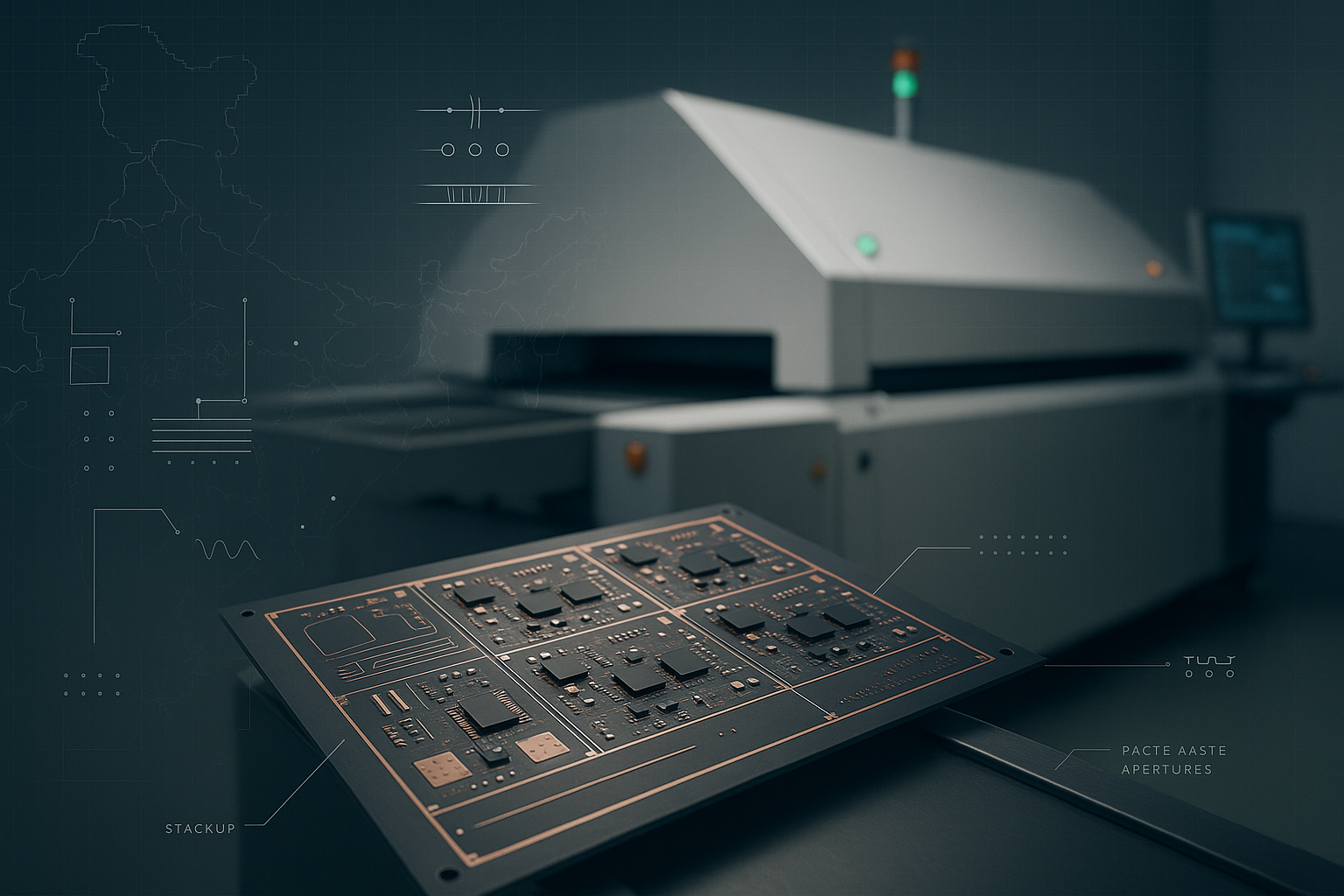
Wave soldering is a technique used to solder through-hole components to guarantee that the solder conforms to the exposed metal surfaces of the components and the board. It passes the PCB across a wave of molten solder, therefore generating strong electrical connections. The basic idea of wave soldering is based on the molten solder wave contacting the underside of the PCB, therefore effectively connecting all the component leads concurrently. Wave soldering mostly uses the conveyor system and the solder wave machine as its equipment.
The solder wave machine comprises a heated reservoir of molten solder and a pump producing a fountain of solder continuously. This wave guarantees soldering of every exposed metallic surface and even coverage. Preheating, fluxing, soldering, and cooling are among the several phases of the soldering process the conveyor system moves the PCBs through. While fluxing cleans and prepares the surfaces for better solder adherence, preheating guarantees that the PCB and components achieve the suitable temperature before soldering. For through-hole components—that is, those with leads passing across PCB holes—wave soldering is especially appropriate.
Commonly found in many electronic gadgets, these parts offer strong mechanical and electrical connections. Among through-hole components are resistors, capacitors, connectors, and some forms of integrated circuits. For mixed-technology boards—where both through-hole and surface-mounted components may be present—this approach is quite efficient for high-volume manufacturing. Reliable and high-quality PCB fabrication process depends on a knowledge of wave soldering and its uses.
The Evolution of Wave Soldering
Rising demand for dependable and efficient PCB assembly in the expanding electronics sector led to wave soldering beginning in the 1950s as a solution. First, the technique was designed to simplify the soldering of mostly used through-hole components at the time. By drastically lowering the time and effort needed for hand soldering, this approach transformed PCB production and guaranteed constant quality and dependability in electrical connections.
Wave soldering technique has experienced significant developments over several decades. Rudimentary wave designs and rudimentary control techniques defined early generations. But as more complicated devices emerged, the technology developed to incorporate sophisticated preheating and fluxing processes, improving solder adherence and lowering flaws. While symmetrical waves improved homogeneity, more developments resulted in the acceptance of asymmetrical wave designs. It improved coverage and reduced solder bridges.
Another major turning point was the wave soldering process's incorporation of Surface Mount Devices (SMDs). Chip waves made it possible to simultaneously solder SMDs and through-hole PCB components. Hence, it provides wave soldering's adaptability and efficiency for mixed-technology boards. These generational advancements have confirmed the importance of wave soldering in contemporary PCB manufacturing. Therefore, it will always be a necessary operation in the manufacture of dependable electronic assemblies.
Key Factors for Optimal Wave Soldering
Among various important aspects, temperature, wave height, and conveyor speed affect optimal wave soldering. Usually between 250 and 260°C, the solder temperature has to be exactly regulated to provide appropriate melting and adhesion without damaging the PCB or components. Wave height must be sufficient to contact the leads and pads sufficiently but not so high as to produce too great soldering flaws. Conveyor speed controls the solder wave's exposure time; too slow might cause overheating and damage while too quick can lead to inadequate soldering.
In wave soldering, flux application is essential since it cleans the PCB and component leads, therefore enhancing solder adherence and avoiding oxidation. Techniques of flux application consist in foam, spray, and wave fluxing. While wave fluxing offers uniform coverage, spray fluxing permits exact control and foam fluxing creates a consistent foam layer. To get best outcomes, every technique has to provide the right flow distribution and volume.
Effective wave soldering depends on good PCB design and component location. Orienting components will help to reduce shadowing effects and guarantee consistent solder distribution. Reliable solder junctions are reached in part by design factors like suitable pad sizes, spacing, and thermal reliefs. Before soldering, making sure components are precisely positioned and aligned helps to improve the PCB assembly's general quality by avoiding flaws.
Generations of Wave Soldering Machines
The evolution of wave soldering machines has seen significant generational advancements, each improving the efficiency and quality of PCB assembly.
- First Generation: Early wave soldering machines used straightforward symmetrical wave patterns. These devices were covered consistently with a single wave of molten solder, but they sometimes produced solder bridges and other flaws. Making sure fundamental functioning and dependability for through-hole components took front stage.
- Second Generation: Better control systems and preheating stages were two second generation improvements that enhanced solder joint quality and less thermal shock to components. Symmetric wave designs persisted, but with improvements in wave stability and flux delivery techniques, more consistent and dependable soldering resulted.
- Third Generation: Third generation came with the switch to asymmetrical wave machines. These devices brought twin waves: a laminar main wave after a chaotic chip wave. Especially for complicated and heavily populated high-frequency PCBs, this invention greatly lowered solder bridges and enhanced the soldering process generally by offering better coverage and penetration.
- Fourth Generation: Surface Mount Devices (SMDs) and chip waves defined the fourth generation. These devices handled both through-hole and surface-mounted components and coupled the advantages of asymmetrical waves. Wave soldering is flexible for mixed-technology boards since the addition of chip waves lets smaller SMDs be effectively soldered alongside conventional through-hole components.
- Fifth Generation: The fifth generation used selective pallet wave soldering—a technique whereby particular PCB portions are selectively exposed to the solder wave. For complicated boards such as rf PCB, including a combination of sensitive components, this method is perfect. It lowers the danger of thermal damage and enables exact soldering of desired locations. Maintaining great dependability and quality criteria, selective pallet wave soldering has extended the use of wave soldering to more specialised and complex PCB designs.
Advantages of Wave Soldering
Wave soldering offers numerous advantages, particularly for through-hole components, making it a preferred method in multilayer PCB.
- Efficiency and Speed: Wave soldering's efficiency and speed rank among its main advantages. Compared to hand soldering or other techniques, this procedure greatly reduces the time needed by simultaneously soldering several components. For big volume manufacturing runs, the constant conveyor system guarantees a simplified process and is hence perfect.
- Reliability: Wave soldering produces solder junctions with a recognized dependability and strength. Strong mechanical and electrical connections are produced by the molten solder wave guaranteeing total coverage and great adherence. The lifetime and performance of electronic equipment depend on this dependability. It reduces the possibility of connection failures and increases general durability.
- Cost-Effectiveness: Especially for mass production, wave soldering is also reasonably affordable. The automated character of the process raises throughput and lowers labour expenses. Furthermore helping to cut total manufacturing costs are the effective use of solder and flux and the lower occurrence of flaws. Wave soldering offers a very cheap way for producers hoping to generate lots of PCBs with constant quality.
Comparing Wave Soldering with Reflow Soldering
Surface-mounted components (SMDs) are soldered onto a printed circuit board (PCB) via reflow soldering. It is done by applying a paste of solder and flux then heating it to melt and form joints. Perfect for through-hole components, wave soldering is passing the PCB over a wave of molten solder.
- Process and Applications: Reflow soldering forms connections by heating the PCB in a reflow oven, melting the solder paste. Usually, it's used for SMDs. Mostly utilised for through-hole components, wave soldering—with its molten solder wave—can also handle some mixed-technology boards.
- Suitability for Different PCBs and Components: Because of its exact control over heating and soldering, reflow soldering is well suitable for PCBs with high density of SMDs. Modern devices including laptops and cellphones often feature it. PCBs with multiple through-hole components would be better suited for wave soldering since it offers strong and dependable junctions for these bigger, more sturdy components.
- Preferred Scenarios: When precision and handling fine-pitch components are absolutely vital, as in consumer electronics with dense SMD layouts, reflow soldering is recommended. Applications needing the strong connection of through-hole components—such as in power supplies, industrial equipment, and some mixed-technology boards—wave soldering is perfect. Every methodology has advantages, hence based on the particular needs of the project, they are complementary techniques in PCB assembly.
Practical Guide to Wave Soldering
Wave soldering is a multi-step process essential for creating reliable connections in PCB assembly. Here is a step-by-step guide to wave soldering:
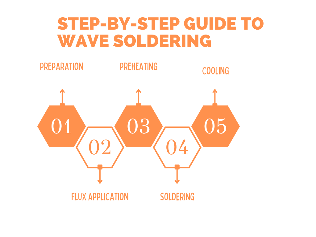
- Preparation: Begin by preparing the PCB, ensuring all components are correctly placed and secured. Check for proper alignment and any potential issues that could affect soldering.
- Flux Application: Flux is applied to the PCB to clean the component leads and pads, promoting better solder adhesion. There are two primary methods:some text
- Foam Fluxing: Uses bubbling air through a liquid flow to create a foam. The PCB goes across the foam, coating its underside. For boards with simple layouts, this approach offers consistent coverage and is best.
- Spray Fluxing: Flux is sprayed finely to cover the PCB. This approach is appropriate for complex or highly populated PCBs. It provides more exact control, enables focused application, and helps to lower excess flux use.
- Preheating: Then the PCB is heated to activate the flux and evaporate any solvents that might be present. This stage also guarantees that the board and parts get the right temperature before the soldering operation, therefore avoiding thermal shock.
- Soldering: Hot solder is applied to link the component leads to the pads on the printed circuit board (PCB) across the solder wave. Controlling the conveyor's speed and wave height helps to guarantee that the soldering is done precisely and fault-free.
- Cooling: After soldering, cooling the printed circuit board (PCB) helps the solder joints to become firm. Regarding joint dependability and thermal stress prevention, appropriate cooling is rather essential.
Types of Solder Used
Most often used solders in wave soldering are lead-free alloys and tin-lead (Sn-Pb) solders. Though it is being phased out for environmental concerns, tin-lead solder—usually with a 63/37 or 60/40 concentration—has remarkable wettability and mechanical strength. Currently the most often used lead-free solders are those with strong mechanical capacity and compliance with environmental rules, including SAC305 (tin-silver-copper).
Ensuring Quality in Wave Soldering
The implementation of tight process controls, the maintenance of equipment calibration, and the elimination of common flaws are all necessary steps in the process of wave soldering quality assurance.
Common Defects and Remedies:
- Solder Bridges: These are the effects of too much solder linking adjacent PCB pads. Potential remedies for optimization include wave height, conveyor speed, and flux application.
- Insufficient Solder: Eventually, insufficient wave contact or flux application could cause this issue to occur. By adjusting the wave parameters and guaranteeing proper preheating, one can solve this issue.
- Cold Joints: These follow from inadequate heat, which produces poor solder flow. One cannot emphasise the need of properly preheating solder and maintaining the temperature steady.
Quality Control Factors:
- Equipment Calibration: Regular calibration of the wave solder machine guarantees consistency in the solder temperature, wave height, and conveyor speed. High-quality solder connections are produced by these elements, all of which are required.
- Process Control: Extremely crucial are monitoring and adjusting the application of flux, preheat temperature, and conveyor speed. Tools that help to preserve process consistency are the application of standard operating procedures (SOPs) and the preservation of thorough records.
Precautions During Manual Wave Soldering:
- Safety Gear: In order to avoid getting burned and being exposed to flux fumes, operators should make sure to use the required safety equipment. It includes goggles and eye protection.
- Consistent Technique: It is helpful to maintain a constant soldering method to achieve uniform solder junctions. This includes maintaining a steady hand movement and finding the optimum soldering angle.
- Ventilation: It is essential to make certain that there is sufficient ventilation in order to remove fumes and to keep the working environment safe.
Conclusion
For through-hole components, wave soldering provides efficiency and speed; for strong, dependable solder junctions, it offers cost-effectiveness for mass production. It is less suited for very complicated PCBs dominated by surface-mount devices (SMDs), or for densely populated PCBs. Mixed-technology boards can also provide difficulties; strict process control is therefore necessary to prevent flaws including cold joins and solder bridges. Meeting particular PCB criteria depends on selecting the correct soldering technique. Reflow soldering is better suited for PCBs with a high density of SMDs, providing exact control and flexibility, even while wave soldering shines in handling through-hole components and high-volume manufacturing.
FAQ's
What is wave soldering?
In PCB manufacture, wave soldering is a technique used effectively to solder through-hole components. To guarantee that the solder conforms to the exposed metal surfaces of the components and the board, it passes the PCB across a wave of molten solder, therefore generating strong electrical connections. Stages ranging from flux application to preheating soldering to cooling comprise the process. Preheating activates the flux and helps to avoid thermal shock; the molten solder wave produces the solder junctions and cleans and ready the surfaces for soldering. Mixed-technology boards and high volume manufacture call for wave soldering.
What are the advantages of wave soldering?
For through-hole components especially, wave soldering has various benefits. It is quite rapid and efficient, able to soldered several components at once, so drastically cutting production time. Strong and dependable solder junctions created offer outstanding mechanical and electrical connections. Because of its automated character, which lowers labor costs and boosts throughput, this approach is also affordable for mass manufacturing. Moreover, wave soldering guarantees constant quality and reduces flaws, which makes it the best option for PCB high-volume production including mixed technology and through-hole components.
How does wave soldering differ from reflow soldering?
Two different PC assembly techniques are wave soldering and reflow soldering. Perfect for through-hole parts, wave soldering is passing the PCB across a wave of hot solder. For big volume manufacturing, it is quite effective; but, it is less suited for densely inhabited SMD boards. Conversely, for mainly SMDs, reflow soldering melts solder paste put to the PCB using a reflow oven. Perfect control and fit for fine-pitch components and intricate layouts make it appropriate. Every technique is specific for different kinds of components and PCB designs; wave soldering favors through-hole and reflow for SMDs.
What factors influence the quality of wave soldering?
Among various elements, solder temperature, wave height, and conveyor speed affect the quality of wave soldering. Good temperature management guarantees strong soldering free from component damage. To get complete soldering without producing flaws, wave height has to be ideal. Conveyor speed controls the length of exposure to the solder wave; too slow can cause overheating while too quick can result in inadequate soldering. Cleaning and preparing surfaces for soldering depend on flux application; methods like foam and spray fluxing impact coverage. Furthermore important to prevent shadowing and guarantee consistent solder distribution are correct PCB design and component location.