Printed Circuit Boards (PCBs) are boards on which the electronic components are mounted and the connections between them are made electrically.
PCBs are commonly made of fiberglass FR4 material, but they also come in other variants like composite epoxy and ceramics. Depending on the rigidity of the base materials there are flexible PCBs, rigid PCBs, and rigid-flex PCBs. For more complex circuits which need a lot of connections between the component's wires, they will have to be routed in multiple layers of copper planes. This is achieved in multi-layer PCBs which come in 4/6/8...and all the way up to 60 layers.
A good PCB should have the following characteristics:
- Good Finishing
- No scratches on the board
- Copper should not be seen
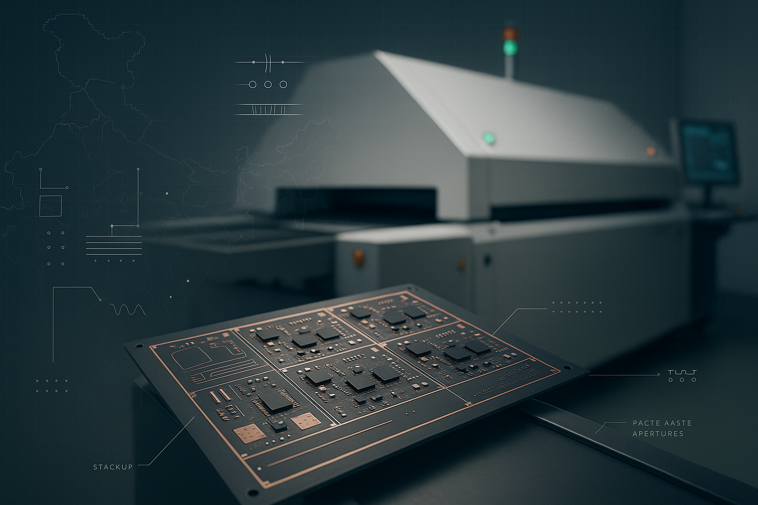
Process OF PCB manufacturing:
Sheet Cutting:
The copper laminate sheet will be cut into the required shape as requested by the customer design.
CNC(Computer Numerical Control) Drilling:
Cut Boards will be drilled in CNC machinesmachine as per the design data for via’s and through hole connections. In case of multilayer pcbs this process is done at a later stage.
PTH(Plating Through Holes):
Drilled holes will go through an electroless chemical treatment process which builds the copper between the top and the bottom layer thus establishing an electrical connection between the two layers of pcb.
Photo Printing (Dry Film):
The design which is photo plotted on a film will be placed on the copper laminate board along with a photo-sensitive material to get imprinted onto the copper board after being exposed to light for a certain amount of time.
Developing:
Only the design being exposed to light will have copper on it whereas the rest of the board where the design is not present will have the dry film.
Photo Printing Inspection:
Design will be inspected for accuracy of printing and any smudges will be inspected on the board.
Tin Plating:
Boards will be dipped in a bath with tin electrodes for an electroplating process which deposits the tin on copper exposedexpose areas. Now the boards are being prepared for the etching process.
Tin Plating Inspection:
Boards will be inspected after plating for any areas which havehas not got sufficient tin plating.
Etching:
Boards will be treated in a chemical process that will remove the copper which is exposed along with dry films. The area which is coated with Tin will be preserved.
Etching Inspection:
Copper etched boards will be checked for over-etching, track cuts etc.
PISM(Photoimageable Solder Masking):
Copper boards will be aligned under the screen and solder mask will be applied on the boards with colour requested by the customer (i.e white, green, red, blue, black), it will then be exposed to a UV light source for curing the paint.
Heat Curing:
Boards are then kept in an industrial oven for a specific time for the ink to cure completely which provides good adhesion to the circuit boards.
HAL (Hot Air Levelling):
Boards after masking will have the circuits printed on it and the component pads are exposed since copper will oxidise very quickly with air, it has been covered with a metal that stops oxidization and also provides good solderability. HAL processes typically use a combination of lead and tin in the 37:63 ratio to be coated on the copper.
Lead Free HAL:
Since the HAL process includes lead which is a heavy metal and most of the modern electronics is manufactured to exclude lead, tin along with silver combination is used in the lead-free HAL process.
Alternately ENIG/ ENIPG or other electroless gold process is also used as a surface finish process to stop oxidation of copper.
FPT(Flying Probe Tester):
Electrical functionality of the PCB will be tested in this machine i.e to make sure that the board does not have any defects and is performing the functions stated by the customer design as per the netlist provided.
Cutting:
CNC Routing:
Boards will be cut as per the shape provided by the customer design using a CNC machine that can achieve complex shapes.
V-Grove:
Boards with just straight-line cuts will be processed in a V-grove machine, typically used in mass production panel format designs.
Packaging:
The boards will be vacuum-packed and are securely covered with bubble wrap and are put inside a box, ready to dispatch to customers.
The above PCB manufacturing process is only a high-level overview and various processesprocess involved in PCB making. This is not an accurate step-by-step process. For a multi-layer pcb there will be additional chemical process steps and vacuum press steps involved to fuse the different layers together.
Different Types of PCB Materials
PCB base materials come in various types other than FR4. Special materials for high-frequency applications are used which are PTFE composites or woven glass hydrocarbons from Rogers, Isola, Nelco are few examples. These materials are optimised for low loss tangents at high frequency and hence suitable for high-frequency systems in radars and other communication devices.
In summary, PCBs are the building blocks in any electronic device. It is found in our day-to-day devices like smartphones, refrigerators, air-conditioners, microwave units, water heaters, and cars without which we can't imagine living. It plays an important role in all our lives and also in the electronics and communications industry on a large basis.